Zappy Module
From Hackstrich
Zappy Module is a board-level module that takes control input via some kind of protocol and outputs signals to zap someone like shock collars do.
Contents
Project Status
- 2016-02-13: Made all Rev003 fixes, need to checklist and do final review tomorrow before sending off.
- 2016-01-01: Put on proper feedback and fixed a backwards diode, now generates good voltage out. Working on setting the duration using a timer instead of number of pulses, not working yet.
- 2015-12-24: Assembled first Rev002 board, semi-working right now. Issues noted below, left off at realizing that R16 is also the wrong value on BOM, so need to fix that to get proper feedback next time and see how it looks after doing that.
- 2015-12-23: Parts are all here including PCBs and magnetics, will be able to work on this over the break.
- 2015-09-13: Sent to OSH Park for manufacturing, ordered magnetics from Coilcraft (plus a couple other xfmrs to try as options).
- 2015-05-25: Completed Rev002 layout, pending final review.
- 2015-05-24: Finished Rev002 schematic, board layout still needs to be done.
- 2015-05-23: Started rev002, got all issues fixed except the medium voltage rail shutdown.
- 2015-05-18: Did a bunch more SPICE analysis on various types/ESRs/capacitance values for the main tank capacitor, found a suitable Digikey electrolytic part that has acceptable parameters.
- 2015-05-10: More characterizing done, found it needs 100uF not 10uF, tacked on an electrolytic for now, will get a 100uF ceramic for further testing. Next steps are to implement the trigger inputs.
- 2015-05-05: Basic I2C functionality implemented and working, can set a power level and number of pulses, though not calibrated to anything yet.
- 2015-04-29: ARM signal is now obeyed, triggering is only possible when ARM is high. Started working on I2C, not working yet.
- 2015-04-24: Assembled logic side of board and threw together some test firmware, basic functionality is all working. Worked on/sorted out pulse shaping with some extra components on the secondary side of the transformer. Next step is to implement I2C.
- 2015-04-22: Assembled analog side of first board, +3.3v and +10v rail are both working fine, as is the cap charging circuitry. started testing HV triggering but really need the logic on the board to test it properly. Next time will assemble logic and throw some test firmware together to sequence charging/triggering.
- 2015-04-21: Boards arrived, ordered parts.
- 2015-03-26: Sent to OSH Park for PCB manufacturing. Still need to order main transformer from Coilcraft and parts from Digikey.
- 2015-03-15: Completed routing board, silkscreen and checklist run done. Waiting 24h for final review and submission to OSH Park.
- 2015-03-08: Finished schematic and BOM, checklisted.
- 2015-03-07: Started putting schematic and BOM together.
- 2015-02-02: Started putting together overall circuit idea.
- 2015-02-01: SPICEd out some ideas.
- 2015-01-29: Captured waveforms of all output levels.
- 2015-01-05: Arranged to borrow a shock collar to characterize the output of it.
- 2013-05: Started throwing ideas around.
Overview
- Main control input via I2C
- ARM signal must be high before zapping is allowed
- Two trigger pin inputs, can program levels for each via I2C then zap with simple "pull pin high" I/O
Theory of Operation
- Input voltage from 3-5V is stepped up to 10V using a boost converter (AZ34063U) to get the intermediary voltage rail
- MCU controls a FET that charges a cap from that rail via a series resistor to control charge rate
- Divider on the cap feeds into an analog pin on the MCU, once the analog pin reaches the desired level the MCU shuts the FET off again
- Once cap is charged, MCU pulses a FET that dumps the charge on the cap through a 1:100 (or so) transformer and to the output
- 0.1-1kV should be achievable via timing the charge FET
- May need a dump resistor if the cap is charged and needs to be discharged without zapping?
- Could use the series charging resistor w/ a different FET to dump the cap through it?
- Don't think this will be required, the charge cycle will only take ~1mS so it will be done right before the trigger, so the cap will never remain charged for long
Protocol
- I2C, default address 0x5F
- All commands follow the basic format of:
- Three magic bytes to ensure no zapping from random probing or bus noise (0x5A, 0x41, 0x50 / Z A P)
- One byte command
- Variable number of one byte arguments
- 0x00 - NOOP
- 0x01 - ZAP
- Arg 1 - Level
- 0-255, volts/2 to output
- Arg 2 - Pulse length
- 0-255, milliseconds to pulse for
- Arg 1 - Level
- 0x02 - SET
- Arg 1 - Channel to set
- 0=A, 1=B
- Arg 2 - Level
- 0-255, volts/2 to output
- Arg 3 - Pulse length
- 0-255, milliseconds to pulse for
- Arg 1 - Channel to set
- 0x03 - ADDR
- Arg 1 - New address to take on
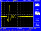
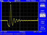
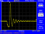
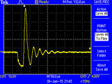
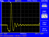
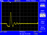
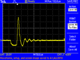
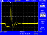
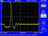
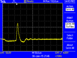
Collar Reversing Waveforms
- All collar output waveforms are through a 1/3 divider, so multiply by 3 to get actual amplitude
- Lowest level (1L) seems to be ~90Vpp, highest seems to be ~450Vpp
- I thought the highest was ~2x that? Need to measure the higher ones again to double check
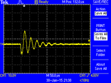
Collar Output - Level 1L
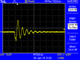
Collar Output - Level 2L
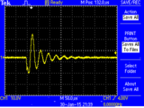
Collar Output - Level 3L
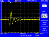
Collar Output - Level 4L

Collar Output - Level 5L
Collar Output - Level 6L
Collar Output - Level 8L
Collar Output - Level 1H
Collar Output - Level 2H
Collar Output - Level 3H
Collar Output - Level 4H
Collar Output - Level 5H
Collar Output - Level 6H
Collar Output - Level 7H
Collar Output - Level 8H


Rev 1 Issues
D1-D3 on BOM only has qty 2- Fixed in Rev002C4 is 0603 on board but 0402 on BOM- Fixed in Rev002Need pulldowns on the FET gates- Fixed in Rev002- Otherwise when programming both trigger/charge can be on at once which pulls lots of current and can blow up parts
Need 33pF (or so) and a diode across the transformer secondary to shape pulses- Added in Rev002+10V rail is ~12V since it's mostly unloaded.- No fix required- This is fine since we want to charge the capacitor faster rather than slower.
Input pins only register as HIGH at 5v, resistors need to be changed to ~800k to make it work at 3.3- Fixed in Rev002- Will change PIC to run at input voltage, which makes 3-5v possible w/ no level shifting
No pullups on the I2C pins (errata clarifies that the docs are wrong when it says they have pullups)- No specific fix required- Don't need built in pullups, the master or board that this plugs into should provide this
Level shifting for I2C doesn't work, need to investigate using a proper level shifter- No specific fix required- Switching to run the PIC at input voltage means no level shifting required
Reservoir capacitor needs to be 100uF (or higher), not 10uF- Fixed in Rev002- Digikey part 732-6415-1-ND has acceptable size, capacitance, ESR (when SPICEd), and cost
Should have a shutdown for the medium rail to save power when idle- Done in Rev002Should have a solder jumper to disable LEDs for power savings- Done in Rev002
Rev 2 Issues
U2 is on BOM but not used- Fixed in Rev003ICs have no pin 1 markings on board- Fixed in Rev003R6, R16 should be 6.8k, BOM has 56k- Fixed in Rev003Pin 2 on U3 should go to the switched AGND not AGND itselfCan't share 10V_ON w/ ICSPCLK, messes up voltage rails badly when programming, swapped TRIG_OUT and 10V_ON on Rev002 #1- Fixed in Rev003C3 should be 330pF, BOM has 30pF- Fixed in Rev003100 is way too big for R1 with the new cap, 22 seems reasonable so far- Fixed in Rev003D4 is backwards- Fixed in Rev003