Difference between revisions of "Zappy Module"
From Hackstrich
| Line 11: | Line 11: | ||
== Overview == | == Overview == | ||
| − | * | + | * Main control input via I2C |
| − | * | + | * ARM signal must be high before zapping is allowed |
| − | + | * Two trigger pin inputs, can program levels for each via I2C then zap with simple "pull pin high" I/O | |
| − | |||
== Theory of Operation == | == Theory of Operation == | ||
* Input voltage from 3-9V is stepped up to 10V using a boost converter (AZ34063U) to get the intermediary voltage rail | * Input voltage from 3-9V is stepped up to 10V using a boost converter (AZ34063U) to get the intermediary voltage rail | ||
| − | |||
* MCU controls a FET that charges a cap from that rail via a series resistor to control charge rate | * MCU controls a FET that charges a cap from that rail via a series resistor to control charge rate | ||
** Divider on the cap feeds into an analog pin on the MCU, once the analog pin reaches the desired level the MCU shuts the FET off again | ** Divider on the cap feeds into an analog pin on the MCU, once the analog pin reaches the desired level the MCU shuts the FET off again | ||
Revision as of 03:21, 9 March 2015
Zappy Module is a board-level module that takes control input via some kind of protocol and outputs signals to zap someone like shock collars do.
Project Status
- 2015-03-08: Finished schematic and BOM, checklisted.
- 2015-03-07: Started putting schematic and BOM together.
- 2015-02-02: Started putting together overall circuit idea.
- 2015-02-01: SPICEd out some ideas.
- 2015-01-29: Captured waveforms of all output levels.
- 2015-01-05: Arranged to borrow a shock collar to characterize the output of it.
- 2013-05: Started throwing ideas around.
Overview
- Main control input via I2C
- ARM signal must be high before zapping is allowed
- Two trigger pin inputs, can program levels for each via I2C then zap with simple "pull pin high" I/O
Theory of Operation
- Input voltage from 3-9V is stepped up to 10V using a boost converter (AZ34063U) to get the intermediary voltage rail
- MCU controls a FET that charges a cap from that rail via a series resistor to control charge rate
- Divider on the cap feeds into an analog pin on the MCU, once the analog pin reaches the desired level the MCU shuts the FET off again
- Once cap is charged, MCU pulses a FET that dumps the charge on the cap through a 1:100 (or so) transformer and to the output
- 0.1-1kV should be achievable via timing the charge FET
- May need a dump resistor if the cap is charged and needs to be discharged without zapping?
- Could use the series charging resistor w/ a different FET to dump the cap through it?
- Don't think this will be required, the charge cycle will only take ~1mS so it will be done right before the trigger, so the cap will never remain charged for long
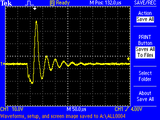
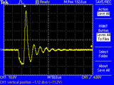
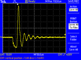
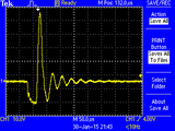
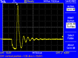
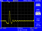
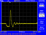
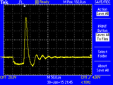
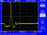
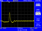
Collar Reversing Waveforms
- All collar output waveforms are through a 1/3 divider, so multiply by 3 to get actual amplitude
- Lowest level (1L) seems to be ~90Vpp, highest seems to be ~450Vpp
- I thought the highest was ~2x that? Need to measure the higher ones again to double check
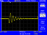
Collar Output - Level 1L
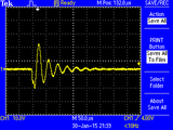
Collar Output - Level 2L
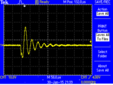
Collar Output - Level 3L
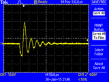
Collar Output - Level 4L

Collar Output - Level 5L
Collar Output - Level 6L
Collar Output - Level 8L
Collar Output - Level 1H
Collar Output - Level 2H
Collar Output - Level 3H
Collar Output - Level 4H
Collar Output - Level 5H
Collar Output - Level 6H
Collar Output - Level 7H
Collar Output - Level 8H


