Difference between revisions of "Zappy Module"
From Hackstrich
| Line 2: | Line 2: | ||
== Project Status == | == Project Status == | ||
| + | * 2015-04-24: Assembled logic side of board and threw together some test firmware, basic functionality is all working. Worked on/sorted out pulse shaping with some extra components on the secondary side of the transformer. Next step is to implement I<sup>2</sup>C. | ||
* 2015-04-22: Assembled analog side of first board, +3.3v and +10v rail are both working fine, as is the cap charging circuitry. started testing HV triggering but really need the logic on the board to test it properly. Next time will assemble logic and throw some test firmware together to sequence charging/triggering. | * 2015-04-22: Assembled analog side of first board, +3.3v and +10v rail are both working fine, as is the cap charging circuitry. started testing HV triggering but really need the logic on the board to test it properly. Next time will assemble logic and throw some test firmware together to sequence charging/triggering. | ||
* 2015-04-21: Boards arrived, ordered parts. | * 2015-04-21: Boards arrived, ordered parts. | ||
| Line 55: | Line 56: | ||
* 0402 pads are too big | * 0402 pads are too big | ||
* No pins on BOM | * No pins on BOM | ||
| − | + | * Need pulldowns on the FET gates | |
| + | ** Otherwise when programming both trigger/charge can be on at once which pulls lots of current and can blow up parts | ||
| + | * Need 33pF (or so) and a diode across the transformer secondary to shape pulses | ||
| + | * +10V rail is ~12V since it's mostly unloaded. | ||
[[Category:Current Projects]] | [[Category:Current Projects]] | ||
Revision as of 04:09, 25 April 2015
Zappy Module is a board-level module that takes control input via some kind of protocol and outputs signals to zap someone like shock collars do.
Contents
Project Status
- 2015-04-24: Assembled logic side of board and threw together some test firmware, basic functionality is all working. Worked on/sorted out pulse shaping with some extra components on the secondary side of the transformer. Next step is to implement I2C.
- 2015-04-22: Assembled analog side of first board, +3.3v and +10v rail are both working fine, as is the cap charging circuitry. started testing HV triggering but really need the logic on the board to test it properly. Next time will assemble logic and throw some test firmware together to sequence charging/triggering.
- 2015-04-21: Boards arrived, ordered parts.
- 2015-03-26: Sent to OSH Park for PCB manufacturing. Still need to order main transformer from Coilcraft and parts from Digikey.
- 2015-03-15: Completed routing board, silkscreen and checklist run done. Waiting 24h for final review and submission to OSH Park.
- 2015-03-08: Finished schematic and BOM, checklisted.
- 2015-03-07: Started putting schematic and BOM together.
- 2015-02-02: Started putting together overall circuit idea.
- 2015-02-01: SPICEd out some ideas.
- 2015-01-29: Captured waveforms of all output levels.
- 2015-01-05: Arranged to borrow a shock collar to characterize the output of it.
- 2013-05: Started throwing ideas around.
Overview
- Main control input via I2C
- ARM signal must be high before zapping is allowed
- Two trigger pin inputs, can program levels for each via I2C then zap with simple "pull pin high" I/O
Theory of Operation
- Input voltage from 3-9V is stepped up to 10V using a boost converter (AZ34063U) to get the intermediary voltage rail
- MCU controls a FET that charges a cap from that rail via a series resistor to control charge rate
- Divider on the cap feeds into an analog pin on the MCU, once the analog pin reaches the desired level the MCU shuts the FET off again
- Once cap is charged, MCU pulses a FET that dumps the charge on the cap through a 1:100 (or so) transformer and to the output
- 0.1-1kV should be achievable via timing the charge FET
- May need a dump resistor if the cap is charged and needs to be discharged without zapping?
- Could use the series charging resistor w/ a different FET to dump the cap through it?
- Don't think this will be required, the charge cycle will only take ~1mS so it will be done right before the trigger, so the cap will never remain charged for long
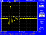
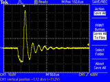
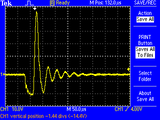
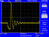
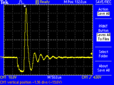
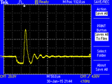
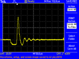
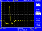
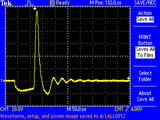
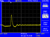
Collar Reversing Waveforms
- All collar output waveforms are through a 1/3 divider, so multiply by 3 to get actual amplitude
- Lowest level (1L) seems to be ~90Vpp, highest seems to be ~450Vpp
- I thought the highest was ~2x that? Need to measure the higher ones again to double check
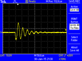
Collar Output - Level 1L
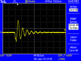
Collar Output - Level 2L
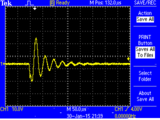
Collar Output - Level 3L
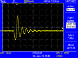
Collar Output - Level 4L

Collar Output - Level 5L
Collar Output - Level 6L
Collar Output - Level 8L
Collar Output - Level 1H
Collar Output - Level 2H
Collar Output - Level 3H
Collar Output - Level 4H
Collar Output - Level 5H
Collar Output - Level 6H
Collar Output - Level 7H
Collar Output - Level 8H


Rev 1 Issues
- D1-D3 on BOM only has qty 2
- 0402 pads are too big
- No pins on BOM
- Need pulldowns on the FET gates
- Otherwise when programming both trigger/charge can be on at once which pulls lots of current and can blow up parts
- Need 33pF (or so) and a diode across the transformer secondary to shape pulses
- +10V rail is ~12V since it's mostly unloaded.